

uwe electronic offers burn-in sockets from Wells-CTI and Sensata – two of the world's leading manufacturers of solder-free contacting solutions for semiconductor reliability testing. The portfolio covers nearly every common package type: from large-area BGA and LGA packages to fine-pitch CSP and FBGA packages, QFN and QFP packages, right down to discrete TO/SOT and SOP/SSOP/TSSOP/TSOP devices. Depending on the package and requirements, different contact principles are used – such as spring contacts (spring probe), buckle-beam contacts, or cantilever contacts – along with different latching types such as open-top, clamshell or compression mounting. All sockets are built for continuous use at high temperature, high cycle counts and – inside the burn-in oven – additionally high humidity, enabling solder-free, reusable contacting across hundreds to thousands of test cycles. Besides the classic burn-in test used to detect early failures, the same sockets are also excellent for device programming prior to soldering onto the PCB.
Series by Package Type
All series are available as PDF datasheets with precise technical data (pitch, pin count, dimensions, temperature range) available. Click an image to open the corresponding datasheet.
BGA – Ball Grid Array
A BGA package has a regular grid of solder balls on its underside that provides both the electrical and the mechanical connection to the PCB. Burn-in sockets for BGA press the device firmly onto a matching field of spring contacts so that every ball is reliably contacted without a soldering process – ideal for devices with a high pin count in a small footprint.
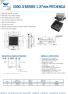
1000-3 Serie
654 Serie
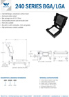
240 Serie
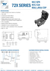
72X Serie
Carrier – Burn-In Carrier Housing
The carrier is not a direct device socket but a housing with a lid that securely holds, mechanically fixes and contacts one or more devices throughout the entire burn-in process. Carriers enable simple, automated transport of the devices through the burn-in oven and into handling systems, without the sensitive leads having to be handled individually.
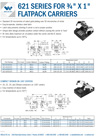
621 Serie
625 Serie
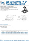
626 Serie
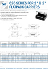
628 Serie
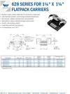
629 Serie
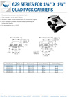
635 Serie
646 Serie
647 Serie
CSP-BGA-QFN – Chip Scale Package / BGA / QFN
This series covers three closely related, particularly compact package types at once: Chip Scale Package (CSP), where the package footprint is barely larger than the die itself, classic BGA, and QFN (Quad Flat No-Leads) without protruding leads. The sockets are designed for very fine pitch dimensions and high contact density, as is typical for modern, space-saving semiconductor packages.
71XP Serie
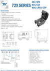
72X Serie
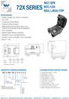
715 Serie
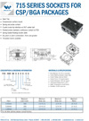
718 Serie
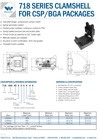
772 Serie
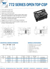
774 Serie
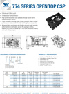
775 Serie
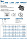
776 Serie

776P Serie
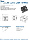
790 Serie
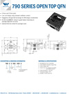
CSP-FBGA – Chip Scale Package / Fine-Pitch BGA
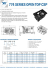
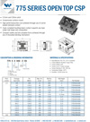
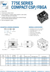
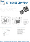
CSP-FBGA is the fine-pitch variant of chip-scale BGA with an even tighter ball grid. This package type is mainly used for highly integrated memory and logic devices, where a very high pin count must be accommodated in the smallest possible space. Accordingly, it places high demands on the socket's positioning accuracy and planarity.
71XP Serie
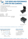
654CSP Serie
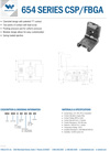
703 Serie
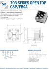
772 Serie
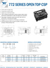
774 Serie
775 Serie
775E Serie
776 Serie

777 Serie
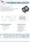
778 Serie
PGA – Pin Grid Array
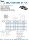
Instead of solder balls, a PGA package carries a grid of pins on its underside that plug into a matching socket matrix. PGA burn-in sockets receive the pins and establish the electrical contact through them – a proven solution for devices with a high pin count where a pluggable rather than a planar contact is preferred.
650 Serie
QFN-LGA – Quad Flat No-Leads / Land Grid Array
QFN packages have no protruding leads, but flat contact pads on the sides of the package and often an additional thermal pad in the center. LGA packages are contacted purely on their underside, with no side leads at all. Both package types are especially flat and compact and are covered together by this socket series.
71XP Serie
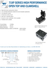
72X Serie
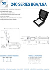
240 Serie
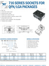
716 Serie
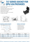
717 Serie
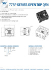
776P Serie
790 Serie
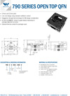
QFP – Quad Flat Package
A QFP package has finely spaced, outward-projecting gull-wing leads on all four sides. This classic, widely used package type requires burn-in sockets with laterally arranged spring contacts that contact the delicate leads gently yet securely.
680 Serie
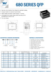
TO-SOT – Transistor Outline / Small Outline Transistor
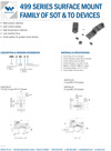
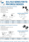
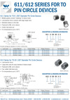
TO and SOT packages are classic designs for discrete semiconductors such as transistors, diodes or small ICs with only a few leads. Despite their simple construction, these devices are produced in very large volumes – accordingly, the matching burn-in sockets are built to be robust and suited to high throughput.
499 Serie
611 Serie
612 Serie
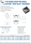
678 Serie
XSOP – (Extended) Small Outline Package
XSOP is an extended variant of the small-outline package with two rows of leads on opposite sides and a higher pin count than a standard SOP. This package type is commonly found on memory devices and compact logic ICs with medium to high pin counts.
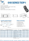
648 Serie
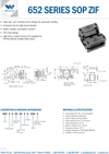
652 Serie
652D Serie
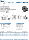
656 Serie
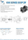
656T Serie
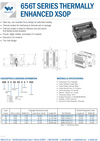
676 Serie
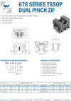
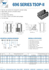
696 Serie
What Is a Burn-In Test?
A burn-in test is a stress test in which electronic devices are exposed simultaneously to elevated temperature and electrical voltage (bias) over a defined period of time. It is based on the so-called bathtub curve of failure rate: newly manufactured semiconductor devices show an elevated probability of failure at the start of their life cycle, caused by latent manufacturing defects – such as oxide defects, weak bond wires, voids in the die-attach layer, or metal migration. The burn-in test accelerates exactly these defects, so that the affected devices can be identified and screened out as early failures ("infant mortality") before they are built into an end product – a key building block for reliable electronics in safety-critical applications.
A burn-in test socket provides the releasable electrical connection between the device under test (DUT) and the burn-in board or oven – entirely without soldering, so the device can be removed and processed further without any trouble after the test. Since a test run typically involves hundreds of devices mounted in parallel on a burn-in board, the socket must withstand not only stable contact quality but above all a high number of insertion and temperature cycles unscathed.
Internationally, the burn-in process is based on standards such as JEDEC JESD22-A108 (Temperature, Bias, and Operating Life) and MIL-STD-883, Method 1015. Typical test parameters for pure early-failure screening burn-in call for a junction temperature Tj of at least 125 °C and a supply voltage at or above the specified maximum, with a test duration of 48 to 168 hours. For further reliability qualification (High Temperature Operating Life, HTOL), the same standards call for test times of 500 to 1,000 hours at the same temperature. Just how much such high-temperature stress anticipates real-world field aging is illustrated by a calculation based on the Arrhenius equation: with a typical activation energy of 0.7 eV, a stress temperature of 125 °C versus an assumed field operating temperature of 55 °C yields an acceleration factor of roughly 78.6 – meaning a 1,000-hour burn-in stress corresponds, mathematically, to roughly nine years of real field use.
How Does a Burn-In Socket Work?
At its core, a burn-in socket consists of three elements: a housing that fixes the socket to the burn-in board and holds or latches the device; the actual contact elements, which electrically connect the device's leads to the board's traces; and a latching or pressure mechanism that presses the device onto the contacts with a defined force and holds it securely for the entire time in the oven.
Latching Types
- Open Top – the device is placed in openly from above and held down by a separate lid or by the burn-in board itself; a simple design, often used with automated placement.
- Clamshell – a hinged lid folds over the device and latches it in place; fast, tool-free loading and unloading by hand.
- Compression mount – the socket is bolted onto the board, and the contacts establish the connection purely through contact pressure; no separate solder joint for the socket itself is needed.
Contact Principles
Depending on the package type, pitch and pin count, different contact technologies are used:
- Spring probe – a classic, spring-loaded contact pin (pogo pin) that compensates for height tolerances and makes contact with a defined force; the standard solution for BGA, LGA and PGA devices.
- Buckle beam – a contact that flexes in a controlled manner when pressed; robust and space-saving, often used in very fine-pitch BGA/FBGA sockets.
- Cantilever (single- or dual-beam) – a spring arm fixed at one end that contacts leads protruding from the side; typical for QFP and QFN packages.
- Pinch contact – two opposing contact springs "clamp" the device from both sides; used among others in certain FBGA series.
Steps in the Burn-In Process
In the typical process flow, the device is placed into the socket and latched, and the loaded socket is permanently mounted on the burn-in board. Several hundred such loaded sockets are pushed together into the burn-in oven and operated there – depending on the test regime – for 48 to 168 hours at a junction temperature typically between 125 °C and 150 °C under electrical bias. Once the test time has elapsed, the board is removed, the devices are electrically retested, defective devices are screened out – and the socket is immediately ready for the next test cycle with new devices.
What Are the Advantages of Burn-In Sockets?
A pluggable burn-in socket is not the only way to contact a device during a burn-in test. In practice, it competes with several alternative contacting and test methods that each bring advantages and drawbacks depending on the application – from simple direct soldering to fundamentally different test philosophies such as system-level test. The comparison below positions the burn-in socket against these alternatives..
Comparison with Similar Contacting Technologies
| Method | Reusability | Advantage over burn-in socket | Disadvantage vs. burn-in socket |
|---|---|---|---|
| Direct soldering of the DUT onto the burn-in board | None – board or device is desoldered or scrapped after the test | Lowest transition resistance and inductance, very close to real operating conditions – advantageous for high-frequency devices | Destructive; every test run requires new soldering/desoldering, significantly higher time and labor cost, no parallel use across changing batches |
| Soldered (solder-mount) socket | Limited – desoldering can deform the socket through thermal stress, solder residue on the contact pins hampers reuse | Tends to have lower upfront cost per socket | Socket replacement only possible via a soldering process, risk to neighboring sockets during reheating, shorter service life compared with solder-free compression mount |
| Elastomer contact | Limited – the silicone interposer is subject to mechanical wear | Very low contact force, shortest signal path, high bandwidth | Generally not designed for the high cycle counts of a burn-in regime (thousands of insertions at high temperature) |
| Wafer-Level Burn-In (WLBI) | Applies to the wafer, not to an individual-chip socket | Screening already occurs before singulation and packaging – defective die incur no packaging cost | Economical only for certain, typically simpler devices (e.g. memory) with sufficient parallelism; complex SoCs are still tested packaged, in a socket |
| System-Level Test (SLT) | Not comparable – a different test principle (functional test in a target-system context) | Covers failures that pure structural test or burn-in do not catch, e.g. hardware/software interactions | Does not replace the thermal-electrical stress screening of burn-in, which specifically provokes early failures |
Core Advantages of the Burn-In Socket
- Solder-free reusability – especially with compression-mount sockets, thousands of devices can be contacted one after another without damaging or replacing the socket itself.
- High degree of parallelization – hundreds of sockets on a single burn-in board enable testing large batch sizes simultaneously at comparatively low cost per device.
- Non-destructive handling – the DUT is subjected to no thermal or mechanical stress from soldering or desoldering when it is loaded or removed.
- Package flexibility – the same board concept can be adapted to different packages (BGA, QFN, QFP, TO-SOT and others) simply by swapping the socket series.
Competing and Complementary Test Trends
Two developments are currently changing the extent to which classic, socket-based burn-in tests are used:
- System-Level Test (SLT) – for complex SoCs with very high transistor counts, structural test and burn-in alone can no longer achieve complete fault coverage; part of the test coverage therefore shifts to SLT in a simulated target system. In application fields where burn-in is required anyway (e.g. automotive), both methods are increasingly combined on the same, high-parallelism test infrastructure rather than replacing one another.
- Adaptive, data-driven test skipping – based on prediction models for the expected failure rate (DPPM) per wafer bin, the share of devices that must go through a full burn-in or SLT run can be significantly reduced for low-risk bins. For already mature, low-risk production lots, this can noticeably cut test effort, while devices from flagged bins continue to be fully tested.
For most packaged, medium- to high-complexity devices, however, the socket-based burn-in test remains the most economical method for detecting early failures, thanks to its combination of solder-free reusability, high parallelism and targeted thermal-electrical stress acceleration.
Application Areas
In the burn-in test segment, uwe electronic's customers are primarily semiconductor manufacturers and specialized test houses. They use the Wells-CTI and Sensata sockets to qualify newly manufactured ICs under realistic thermal and electrical stress before the devices are shipped. Specifically, these test runs follow the requirements of JEDEC JESD22-A108 and MIL-STD-883, Method 1015: for pure early-failure screening, junction temperatures Tj ≥ 125 °C at a supply voltage at or above the maximum value are applied for test times of 48 to 168 hours; for further High-Temperature-Operating-Life qualification (HTOL), the test time at the same temperature extends to 500 to 1,000 hours. These times multiply with the number of parallel test sites: a single burn-in socket must reliably withstand numerous such cycles with changing devices over its entire service life, without its contact resistance measurably deteriorating.
Because the same contact technology enables precise, repeatable and solder-free connections, the sockets are also used extensively for device programming prior to soldering onto a PCB. Here, the sockets are mainly used by customers in embedded technologies, laser technology, automotive and aerospace, where firmware or calibration data must be written to the chip securely and reproducibly before assembly.
Quality Features of Wells-CTI and Sensata Sockets
Burn-in sockets from Wells-CTI and Sensata are characterized by very high durability – even under demanding ambient conditions such as sustained high temperature or high humidity, as typically found in burn-in ovens. This makes the sockets a robust choice for continuous use in production test setups:
- High cycle endurance – designed for a very large number of contact cycles without a significant rise in contact resistance.
- Temperature resistance – materials and contact springs are designed for continuous operation at elevated burn-in temperatures.
- Humidity resistance – stable contact quality even at high humidity inside the oven.
- Broad package portfolio – matching series for nearly every common package, from discrete TO devices to large BGAs.
Package Types at a Glance
Wells-CTI and Sensata offer matching burn-in socket series for every common package type. The table below gives a brief overview of the package types before the next section lists all available series per package type with datasheet.
| Package type | Full term | Typical contacting |
|---|---|---|
| BGA | Ball Grid Array | Grid of solder balls on the underside of the package |
| Carrier | Burn-in carrier housing | Holder for device(s) including lid, for oven transport |
| CSP-BGA-QFN | Chip Scale Package / BGA / QFN (combined) | Fine-pitch balls or contact pads at chip scale |
| CSP-FBGA | Chip Scale Package / Fine-Pitch BGA | Very tightly spaced ball grid |
| PGA | Pin Grid Array | Grid of pins |
| QFN-LGA | Quad Flat No-Leads / Land Grid Array | Flat contact pads with or without side leads |
| QFP | Quad Flat Package | Protruding gull-wing leads on all four sides |
| TO-SOT | Transistor Outline / Small Outline Transistor | A few leads brought out to the side |
| XSOP | (Extended) Small Outline Package | Two rows of side leads, extended pin count |
Products on Request
Beyond the standard Wells-CTI range shown above, we can source additional, more specialized series for QFP as well as FBGA/CSP/BGA/LGA packages on request. These series are not part of the regular range shown on this page, but are available through uwe electronic on demand. If you're interested, please get in touch with us directly.
QFP Sockets – additional series on request
| Series | Pitch | Max. package size / pins | Contact type |
|---|---|---|---|
| 3000 Series | 0.4–0.8 mm | 28×28 mm, 32–208 pins | Open top, single-beam cantilever |
| 680H Series | 0.4–0.8 mm | 28×28 mm, 48–176 pins | Top-loaded, dual-beam cantilever |
| 680HA Series | 0.4–0.8 mm | 28×28 mm, 48–176 pins | Top-loaded, dual-beam cantilever |
| CQF Series | 0.4–0.8 mm | 24×24 mm, 64–176 pins | Side-loaded, dual-beam cantilever |
FBGA / CSP / BGA / LGA Sockets – additional series on request/h3>
| Series | Pitch | Contact type | Note |
|---|---|---|---|
| 715P Series | 0.4–1.27 mm | Spring probe | Compression mount |
| 718P Series | 0.4–1.27 mm | Spring probe | Compression mount |
| 773 Series | 0.4–1.27 mm | Buckle beam | – |
| 892 Series | 0.4–1.27 mm | Buckle beam | Clamshell |
| CBG Series | 0.4–1.27 mm | Pinch | Through-hole mount |
| FBGA Series | 0.4–1.27 mm | Pinch | Through-hole mount |
| Q118 / Q318 Series | 0.4–1.27 mm | Spring probe | Clamshell |
| Q323 Series | 0.4–1.27 mm | Spring probe | Clamshell |
| Q340 Series | 0.4–1.27 mm | Spring probe | Clamshell |
| 859 Series | 0.4–1.27 mm | Buckle beam / spring probe | Clamshell, for large BGA/LGA (35×35–65×65 mm) |
| 861 Series | 0.4–1.27 mm | Buckle beam / spring probe | Clamshell, for large BGA/LGA (35×35–65×65 mm) |
| 863 Series | 0.4–1.27 mm | Buckle beam / spring probe | Clamshell, for large BGA/LGA (35×35–65×65 mm) |
| 869 Series | 0.4–1.27 mm | Buckle beam / spring probe | Clamshell, for large BGA/LGA (35×35–65×65 mm) |
FAQ
What is a burn-in test socket?
A burn-in test socket is a solder-free contacting solution that electrically connects a semiconductor device to the test system or burn-in board during a burn-in test – a long-duration test at elevated temperature and voltage.
For which package types are burn-in sockets available?
uwe electronic offers burn-in sockets from Wells-CTI and Sensata for the package types BGA, Carrier, CSP-BGA-QFN, CSP-FBGA, PGA, QFN-LGA, QFP, TO-SOT and XSOP, each in several series for different pitches and pin counts.
Can burn-in sockets also be used for device programming?
Yes. The same sockets are excellent for programming devices before they are soldered onto a PCB, for example in embedded technologies, laser technology, automotive and aerospace.
How long does a burn-in test take?
Depending on the test regime and underlying standard (JEDEC JESD22-A108, MIL-STD-883 Method 1015), a pure early-failure screening burn-in typically takes 48 to 168 hours at a junction temperature of at least 125 °C. For further HTOL qualification, test times of 500 to 1,000 hours are common.
How often can a burn-in socket be reused?
Solder-free, compression-mounted sockets are rated for several thousand insertion and temperature cycles and can be fitted with new devices again and again without tools or a soldering process. This makes them clearly different from directly soldered devices or soldered sockets, which must be re-soldered or desoldered every time they are replaced.
Does system-level test (SLT) replace the classic burn-in socket?
No. SLT is a complementary test method that covers the fault space that structural test and burn-in do not. For applications that require a burn-in test anyway (e.g. automotive), both methods are increasingly combined on the same, highly parallel test infrastructure – the burn-in socket remains the basis for the thermal-electrical stress acceleration.
What does "products on request" mean?
Beyond the standard Wells-CTI range shown on this page, we can source additional, more specialized series for QFP as well as FBGA/CSP/BGA/LGA packages. These are not part of the regular range, but are available through us on demand – if you're interested, please get in touch with us directly.
What is the lead time for burn-in sockets?
Standard requests typically take 1–4 weeks; custom designs take correspondingly longer.
Technical FAQ: Electrical, Mechanical, Thermal & Selection
The following questions are aimed at engineering and procurement teams and go deeper into electrical parameters, mechanical service life, thermal behavior, and how to choose the right series.
Electrical Properties
How high is the maximum contact resistance and how stable does it remain over its service life?
Typical initial values are below 10–50 mΩ per contact, depending on contact geometry (cantilever, buckle beam, spring probe) and plating (usually gold over nickel). Over the service life, the resistance rises slightly due to contact wear, oxidation and thermal cycling; the stated maximum cycle count generally refers to exactly the point at which the resistance exceeds the specification limit.
What current is permitted per contact?
The current is usually specified so that it exceeds the requirements of the device under test, i.e. the socket is generally not the limiting factor – the device itself is. At high continuous currents (power devices), derating at rising ambient temperature must be observed, since contact resistance and self-heating reinforce each other (thermal-runaway risk during burn-in lasting hours to days).
Insulation voltage between adjacent contacts?
Typical figures are around 1000 VAC (RMS) for 1 minute as a dielectric test value. At very fine pitch (0.35–0.4 mm), the practically usable safety clearance shrinks, which is why fine-pitch series tend to be specified and tested more conservatively.
High-frequency behavior (inductance, crosstalk)?
For logic devices with high clock rates, short contact lengths and low inductance are critical – spring probe and buckle-beam contacts generally perform better here than long cantilever contacts. For specific insertion-loss/crosstalk values, refer to the respective datasheet or request a simulation – this is rarely given as a blanket figure in series overviews.
Mechanical & Service Life
How many cycles does the socket withstand?
A common rating is up to 10,000 insertions/withdrawals as the service-life rating. In practice, the number of cycles actually achieved depends heavily on handling (manual vs. automated), the cleanliness of the test environment, and the package material (rough vs. smooth leads).
Insertion force – ZIF or force-actuated?
Many socket series for SOP, SSOP, TSSOP and TSOP packages are built as open-top ZIF designs – the device is inserted with zero force, and contact pressure is only generated when the lid/actuator closes. This protects the package leads and is a prerequisite for automated loading/unloading.
Actuation – manual, pneumatic, automated?
Standard sockets have a manually actuated lid/lever. For handler integration, pneumatic or motorized actuator variants are available – this is usually a special version or option that must be requested separately and rarely appears in the standard series table.
Suitability for automated handlers?
Yes, especially the ZIF open-top designs are built for pick-and-place compatibility. Key points to clarify: overall height, actuator force and the control interface of the specific handler – this should be coordinated on a project-specific basis.
Thermal
What temperature range does the socket body withstand?
Standard plastic housings are usually specified for −55 °C to +150 °C up to +155 °C. High-temperature variants with other plastics/sealings (e.g. epoxy or Parylene sealing) can go higher; this is always series-dependent and should be checked in the datasheet.
Heat dissipation from the package?
For pure test/burn-in sockets, heat dissipation is generally not the socket's primary task – Thermal Control Units (TCUs) are provided for that purpose and combined with the socket. Some series, however, have a specifically thermally enhanced coupling built in ("thermally enhanced").
Effect of contact resistance on self-heating?
During long burn-in cycles (hours to days) under continuous current, contact resistance can measurably contribute to the socket's self-heating. This is why lower-resistance contact variants (buckle beam instead of single-beam cantilever) are often used for power burn-in.
Compatibility & Selection
Which series fits which package/pitch?
This is the classic first question – the answer follows directly from the series table: package type (QFP/QFN/SOP/TSOP/BGA) and pitch determine the broad series selection, while pin count and maximum package size determine the specific variant within the series.
Does the socket match the PCB footprint?
Here, the hole pattern, solder-pad layout and, where applicable, through-hole vs. compression mounting of the socket must be matched against the customer's board layout – when in doubt, it's advisable to request the package drawing or footprint drawing.
Adapters for special packages?
Yes, this is standard practice – package adapters are available that map a non-standard package onto a standard socket platform. This reduces development time compared with a fully custom new design.
Is custom manufacturing possible?
Yes, custom socket development is offered when no standard series fits – usually with a longer lead time and minimum order quantities.
Procurement & Practice
Is it possible to replace individual contact pins?
Yes, for many series – this is precisely the advantage over soldered connections: worn individual contacts can be replaced without replacing the entire socket, which significantly lowers the total cost of ownership.
Certifications for automotive/medical?
This needs to be clarified separately depending on the application – blanket certification statements are not listed in general series tables; it's always worth asking a targeted question naming the target application.
Burn-in socket vs. pure test socket – when to use which?
Burn-in sockets are designed for long dwell times under continuous current/temperature (hours to days) and are used for 100% burn-in requirements (automotive, medical, aerospace/defense). Pure test sockets are optimized for short, frequent insertion cycles in functional test/characterization. Some applications deliberately switch from 100% burn-in to sample-lot burn-in in order to lower test costs without significantly compromising reliability.
Find the Right Burn-In Socket
Not sure which series fits your device, pitch and temperature profile? We offer burn-in sockets from Wells-CTI and Sensata and support you from initial selection through to custom adaptation.
Jetzt Kontakt aufnehmen